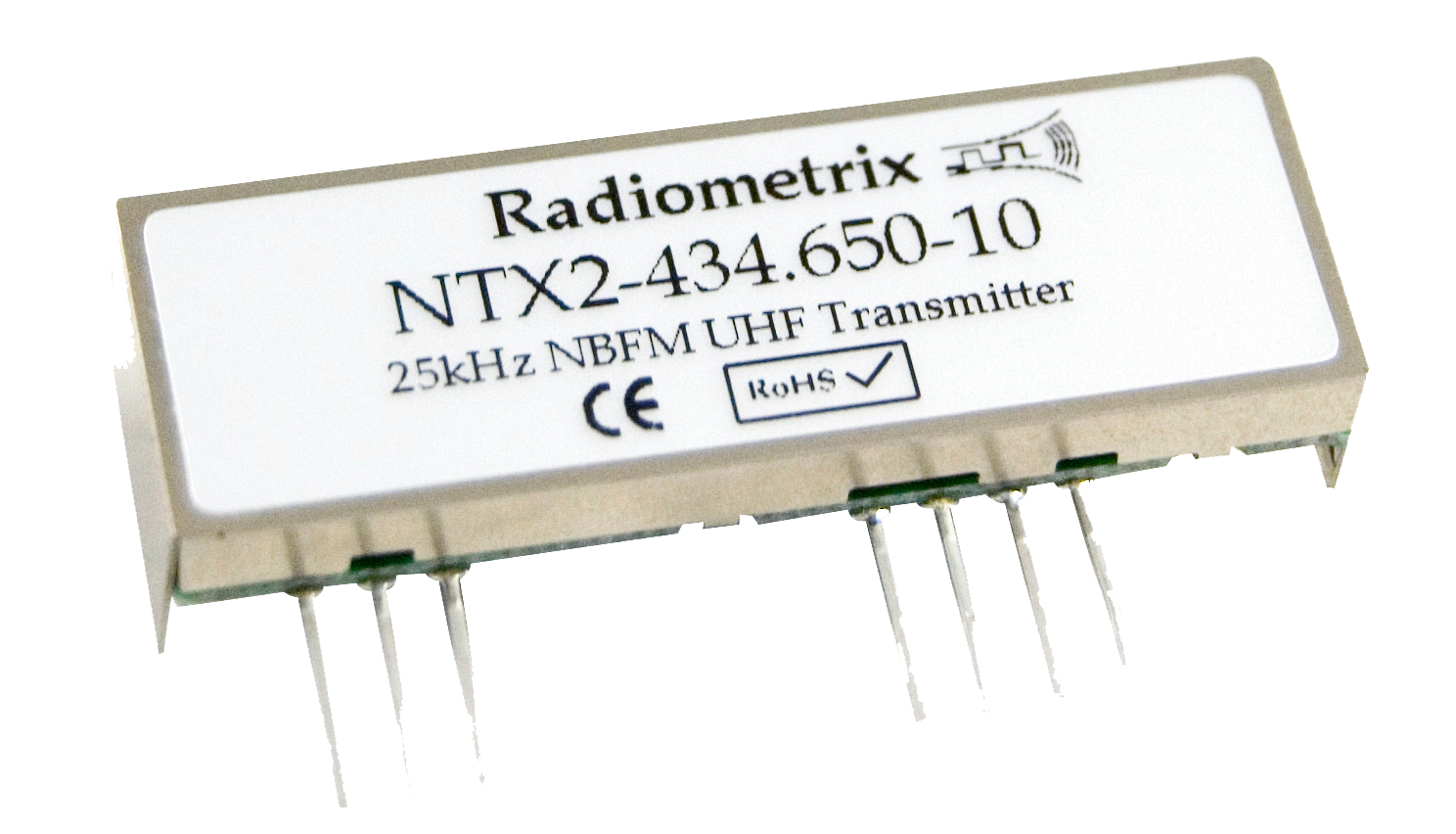
NTX2/NRX2

UHF Narrow Band FM Transmitter and Receiver

The NTX2 transmitter and NRX2 receiver offer a low power, reliable data link in a Radiometrix SIL standard pin out and foot print. This makes the NTX2/NRX2 pair ideally suited to those low power applications where existing single frequency wideband UHF modules have insufficient range.


Figure 1: NRX2-434.65-10 and NTX2-434.65-10

Features

  • Conforms to ETSI EN 300 220-3 (radio) and EN 301 489-3 (EMC)
  • Standard frequencies: 434.075MHz, 434.650MHz and 458.700MHz
  • Custom frequencies available in 433MHz (EU) and 458MHz (UK) band
  • Data rates up to 10kbps
  • Usable range over 500m
  • 25kHz Channel spacing
  • Feature-rich interface (RSSI, analogue and digital baseband)
  • Longer range compared to Wide Band FM modules

Available for licence-exempt operation in the 433MHz (EU) and 458MHz (UK) bands, the NTX2 & NRX2 modules combine effective screening with internal filtering to minimise spurious radiation and susceptibility thereby ensuring EMC compliance. They can be used in existing low data rate (<10kbps) applications where the operating range of the system using TX2 transmitter and RX2 receiver need to be extended. They are particularly suitable for point-to-point and point-to-multipoint wireless links where longer ranges are required at low data rates. Applications include sensor nodes, EPOS and inventory tracking, remote industrial process monitoring, telemetry, telecommand and telecontrol. Because of their small size and low power consumption, both modules are ideal for use in battery-powered portable applications such as handheld terminals.


Applications

  • Handheld terminals
  • EPOS and inventory tracking
  • Remote industrial process monitoring
  • Data loggers
  • Industrial telemetry and telecommand
  • In-building environmental monitoring and control
  • Vehicle and building security and fire alarms
  • Vehicle data up/download

Technical summery

Transmitter - NTX2

  • 3 stage crystal controlled VCXO
  • Supply 2.9V - 15V @ 18mA (internal 2.8V voltage regulator)
  • Data bit rate: 10kbps max.
  • Transmit power: +10dBm (10mW)

Receiver - NRX2

  • Double conversion FM superhet
  • SAW band pass filter, image rejection: 50dB
  • Intermediate Frequencies (IF): 21.4MHz, 455kHz
  • Supply range: 2.9V - 15V @ 14mA (internal 2.8V voltage regulator)
  • Data bit rate: 10kbps max.
  • Receiver sensitivity: -118dBm (for 12dB SINAD)
  • Receiver sensitivity: -112dBm (for 1ppm BER)
  • Local Oscillator (LO) re-radiation: <-60dBm
  • Adjacent Channel: -70dBm
  • Blocking: -84dB

Evaluation Platform: Universal Evaluation kit or Narrow Band Evaluation Kit

Functional description

The NTX2 transmitter consists of a Frequency Modulated (FM) Voltage Controlled Crystal Oscillator (VCXO) feeding a frequency multiplier with two stage amplifier and RF filter. Operation can be controlled by the EN (Enable) line, the transmitter achieving full RF output typically within 5ms of this line being pulled high. The RF output is filtered to ensure compliance with the appropriate radio regulations and fed to the 50W antenna pin.
The NRX2 module is a double conversion NBFM superhet receiver capable of handling data rates of up to 10kbps. It will operate from a supply of 2.9V to 15V and draws 14mA when receiving. A signal strength (RSSI) output with greater than 60dB of range is provided. The SIL style NRX2 measures 47 x 17 x 8 mm excluding the pins.

NTX2 Transmitter


Figure 2: NTX2 block diagram


Figure 3: NTX2 Footprint

Pin Description

Pin
Name
Function
1 & 3 Vcc RF ground is internally connected to the module screen and pin 6 (0V). These pins should be directly connected to the RF return path - e.g. coax braid, main PCB ground plane etc.
2 RF out 50Ω RF output to the antenna
4 EN Pull high to enable Transmitter (3V CMOS logic)
5 Vcc 2.9 - 15V DC power supply
6 0V Ground
7 TXD DC coupled input for 3V CMOS logic. Rin = 100kΩ

NOTES:

1. EN pin should not be left floating
2. Pinout footprint is as TX1H.
3. Compatible with RX2M, RLC2 and NRX2

NRX2 receiver


Figure 4: NRX2 block diagram


Figure 5: NRX2 Footprint

Pin Description

Pin
Name
Function
1 RF in 50Ω RF input from the antenna
2 RF GND RF Ground is internally connected to the module screen and pin 4 (0V). These pins should be directly connected to the RF return path - e.g. coax braid, main PCB ground plane etc
3 RSSI Received Signal Strength Indicator with >60dB range.DC level between 0.5V and 2V
4 0V Ground
5 Vcc 2.9 - 15V DC power supply
6 AF 500mVpk-pk audio. DC coupled, approx 0.8V bias
7 RXD Received Data output from the internal data slicer. The data is squared version of the Audio signal on pin 6 and is true data, i.e. as fed to the transmitter. Output is "open-collector" format with internal 10kΩpull-up to Vcc (pin 5). Suitable for bi-phase codes

NOTES:
1. Pinout is as our wideband RX2A receiver

Absolute maximum ratings

Exceeding the values given below may cause permanent damage to the module.

Operating temperature  -10*C to +60*C
Storage temperature -30*C to +70*C

NTX2
Vcc, TXD (pins 5,7):            -0.3V to +16.0V
En (pin 4):                          -0.3V to +Vcc V
RF out (pin 2):                    *50V @ <10MHz, +20dBm @ >10MHz

NRX2
Vcc, RXD (pins 7,9):           -0.3V to +16.0V
En, RSSI, AF (pins 4,5,8):   -0.3V to +Vcc V
RF in (pin 1):                      *50V @ <10MHz, +13dBm @ >10MHz

Performance specifications: NTX2 transmitter

(Vcc = 3V / temperature = 20°C unless stated)

General Pin min. typ. max. units notes
DC supply
Supply voltage
5
2.9
3.0
15
V
TX Supply current
5
-
18
-
mA
Antenna pin impedance
2
-
50
-
Ω
RF
RF centre frequency
MHz
1
NTX2-434.650-10
-
434.65
-
NTX2-434.075-10
-
434.075
-
NTX2-458.700-10
-
458.700
-
Channel spacing
-
25
-
kHz
Number of channels
-
1
-
RF power output
2
+9
+10
+11
dBm
2
Spurious emissions
2
-
-
-40
dBm
Adjacent channel TX power
2
-
-37
-
dBm
Frequency accuracy
-2.5
-
+2.5
kHz
3
FM deviation (peak)
±2.5
±3
±3.5
kHz
4
Baseband
Modulation type
-
FSK
-
F3D
Modulation bandwidth @ -3dB
0
-
5
kHz
TXD input level (logic low)
7
-
0
-
V
5
TXD input level (logic high)
7
-
3.0
-
V
5
Distortion
TBA
%
6
Dynamic timing
TX select to full RF
-
-
5
ms

Notes:  1. Available in 25kHz channel steps on other custom frequencies in 433MHz/458MHz band
2. Measured into 50Ω resistive load.
3. Total over full supply and temperature range.
4. With 0V - 3.0V modulation input.
5. To achieve specified FM deviation.
6. For 1Vpk-pk signal biased at 1.4V

Performance specifications: NRX2 receiver

(Vcc = 3V / temperature = 20°C unless stated)

General Pin min. typ. max. units notes
DC supply
Supply voltage
1
2.9
3.0
15
V
Supply current
1
-
14
-
mA
RF/IF
RF centre frequency
1, 6
MHz
NRX2-434.650-10
-
434.65
-
NRX2-434.075-10
-
434.075
-
NRX2-458.700-10
-
458.700
-
RF sensitivity @ 12dB (S+N)/N
1, 6
-
-118
-
dBm
RF sensitivity @ 1ppm BER
1, 7
-
-112
-
dBm
RSSI threshold
3
-
-125
-
dBm
1
RSSI range
3
-
55
-
dB
1
IF bandwidth
TBA
-
Blocking
1
-
84
-
dB
Image rejection
1
-
55
-
dB
Adjacent channel rejection
1
-
70
-
dB
Spurious response rejection
1
-
55
-
dB
LO re-radiation
1
-
-
-60
dBm
2
Baseband
Baseband bandwidth @ -3dB
6
0
-
5
kHz
1
AF level
6
-
500
-
mVP-P
3
DC offset on AF out
6
-
0.8
-
V
Distortion on recovered AF
6
-
TBA
-
%
Dynamic timing
Power up with signal present
Power up to valid RSSI
5, 3
-
3
-
ms
Power up to valid AF
5, 6
-
2
-
ms
Power up to stable data
5, 7
-
TBA
10
ms
Signal applied with supply on
Signal to valid RSSI
1, 3
-
2
-
ms
Signal to valid AF
1, 6
-
1
-
ms
Signal to stable data
1, 7
-
TBA
5
ms
4
Time between data transitions
7
0.1
-
TBA
m

Notes:  1. See applications information for further details.
2. Exceeds EN/EMC requirements at all frequencies.
3. For received signal with ±3kHz FM deviation.
4. For 50:50 mark to space ratio (i.e. squarewave)

Applications information

Power supply requirements

Both modules have built-in regulators which deliver a constant 2.8V to the module circuitry when the external supply voltage is 2.9V or greater, with 40dB or more of supply ripple rejection. This ensures constant performance up to the maximum permitted rail, and removes the need for external supply decoupling except in cases where the supply rail is extremely poor (ripple/noise content >100mVpk-pk).

The Enable pin allows the TX module to be turned on or off under 3Vlogic control with a constant DC supply to the Vcc pin. The module current in power-down mode is less than 1mA.

The Enable pin should be tied directly to the Vcc pin if this facility is not required.

TX modulation requirements

The module is factory-set to produce the specified FM deviation with a TXD input to pin 7of 3V amplitude, i.e. 0V "low", 3V "high

If the data input level is greater than 3V, a resistor must be added in series with the TXD input to limit the modulating input voltage to a maximum of 3V on pin 7. TXD input resistance is 100kW to ground, giving typical required resistor values as follows:

Vcc      Series resistor
<3V            -
3.3V         10kΩ
5V            68kΩ
9V            220kΩ

NRX2 Received Signal Strength Indicator (RSSI)

The NRX2 receiver incorporates a wide range RSSI which measures the strength of an incoming signal over a range of 55dB or more. This allows assessment of link quality and available margin and is useful when performing range tests.

The output on pin 3 of the module has a standing DC bias of <0.5V with no signal, rising to 2V at maximum indication..

Typical RSSI characteristic is as shown below:


Figure 6: RSSI response curve

Expected range

Predicting the range obtainable in any given situation is notoriously difficult since there are many factors involved. The main ones to consider are as follows:

  • Type and location of antennas in use
  • Type of terrain and degree of obstruction of the link path
  • Sources of interference affecting the receiver
  • "Dead" spots caused by signal reflections from nearby conductive objects
  • Data rate and degree of filtering employed

Data formats and range extension

The NTX2's TXD input is normally driven directly by logic levels but will also accept analogue drive (e.g. 2-tone signalling). In this case it is recommended that TXD (pin 7) be DC-biased to 1.2V approx. with the modulation ac-coupled and limited to a maximum of 2Vp-p to minimise distortion over the link. The varactor modulator in the NTX2 introduces some 2nd harmonic distortion which may be reduced if necessary by predistortion of the analogue waveform.

Although the modulation bandwidth of the NTX2 extends down to DC as does the NRX2 it is not advisable to use data containing a DC component. This is because frequency errors and drifts between the transmitter and receiver occur in normal operation, resulting in DC offset errors on the NRX2's audio output.

The NRX2 in standard form incorporates a low pass filter with a 5kHz nominal bandwidth. In conjunction with similar filtering in the NTX2 an overall system bandwidth of 5kHz is obtained. This is suitable for transmission of data at raw bit rates up to 10kbps.

Antenna requirements

Three types of integral antenna are recommended and approved for use with the module:

A) Whip: This is a wire, rod, PCB track or combination connected directly to RF pin of the module. Optimum total length is 16cm (1/4 wave @ 433MHz). Keep the open circuit (hot) end well away from metal components to prevent serious de-tuning. Whips are ground plane sensitive and will benefit from internal 1/4 wave earthed radial(s) if the product is small and plastic cased

B) Helical: Wire coil, connected directly to RF pin, open circuit at other end. This antenna is very efficient given it's small size (20mm x 4mm dia.). The helical is a high Q antenna, trim the wire length or expand the coil for optimum results. The helical de-tunes badly with proximity to other conductive objects.

C) Loop: A loop of PCB track tuned by a fixed or variable capacitor to ground at the 'hot' end and fed from RF pin at a point 20% from the ground end. Loops have high immunity to proximity de-tuning.

Whip
Helical
Loop
Ultimate performance
***
**
*
Easy of design set-up
***
**
*
Size
*
***
**
Immunity proximity effects
*
**
***
Range open ground to similar antenna
500
200
100

The antenna choice and position directly controls the system range. Keep it clear of other metal in the system, particularly the 'hot' end. The best position by far, is sticking out the top of the product. This is often not desirable for practical/ergonomic reasons thus a compromise may need to be reached. If an internal antenna must be used, try to keep it away from other metal components, particularly large ones like transformers, batteries and PCB tracks/earth plane. The space around the antenna is as important as the antenna itself.


Figure 7: Antenna types

Module mounting considerations

The modules may be mounted vertically or bent horizontal to the motherboard. Note that the components mounted on the underside of the NTX2 and NRX2 are relatively fragile - avoid direct mechanical contact between these and other parts of the equipment if possible, particularly in situations where extreme mechanical stresses could routinely occur (as a result of equipment being dropped onto the floor, etc).

Good RF layout practice should be observed. If the connection between module and antenna is more than about 20mm long use 50W microstrip line or coax or a combination of both. It is desirable (but not essential) to fill all unused PCB area around the module with ground plane.

Variants and ordering information

The NTX2 transmitters and NRX2 receivers are manufactured in the following variants as standard:

At 434.65MHz: NTX2-434.65-10 - Transmitter
NRX2-434.65-10 - Receiver
At 434.075MHz: NTX2-434.075-10 - Transmitter
NRX2-434.075-10 - Receiver
At 458.700MHz NTX2-458.700-10 - Transmitter
NRX2-458.700-10 - Receiver

Other frequency variants can be supplied to individual customer requirements in the 433MHz (European) and 458MHz (UK) licence exempt bands

Limitation of liability

The information furnished by Radiometrix Ltd is believed to be accurate and reliable. Radiometrix Ltd reserves the right to make changes or improvements in the design, specification or manufacture of its subassembly products without notice. Radiometrix Ltd does not assume any liability arising from the application or use of any product or circuit described herein, nor for any infringements of patents or other rights of third parties which may result from the use of its products. This data sheet neither states nor implies warranty of any kind, including fitness for any particular application. These radio devices may be subject to radio interference and may not function as intended if interference is present. We do NOT recommend their use for life critical applications.
The Intrastat commodity code for all our modules is: 8542 6000.

R&TTE Directive

After 7 April 2001 the manufacturer can only place finished product on the market under the provisions of the R&TTE Directive. Equipment within the scope of the R&TTE Directive may demonstrate compliance to the essential requirements specified in Article 3 of the Directive, as appropriate to the particular equipment.
Further details are available on The Office of Communications (Ofcom) web site:
Licensing policy manual