CTA88
8 bit Address - 8 bit Data encoder/decoder
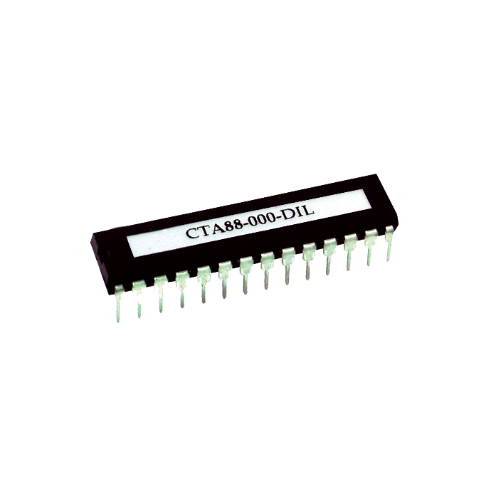
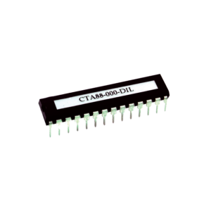
CTA88 is an 8 bit address, 8 bit data encoder and decoder combined in a single IC. This device is intended to be used with ISM band telemetry modules and can be operated in either Encode or Decode mode.
CTA88 uses 1kbps differential Manchester bit balancing with preamble and checksum. It permits a simple, one way link to be established, for simple remote control applications, with a minimum of effort and no customer software input. CTA88 is available in 28pin SO and DIL packages.
Figure 1: CTA88 in 28 pin DIL package
Features
- Operating voltage (temperature):
4.0V-5.5V for standard version (-40°C to +125°C)
2.0V-5.5V for low voltage version (-40°C to +85°C) - Draws <2mA without external load
- 8 bit address and 8 bit data
- 256 different remotes with 8 controls each
- Single packetised transmission for fast activation
- Maximum usuage of the range capability of an RF module
- Adequate preamble to settle data slicer in the receiver
- Extra wake up preamble to allow for transmitter power up time requirements
- Differential Manchester encoding of address, data and checksum
- Synchronisation codes and checksum to reduce false triggering on noise
- Suitable to be used with Narrow Band FM radio modules
- Ceramic resonator or crystal oscillator up to 20MHz
- Data rate up to 5.6kbps
- Minimum external component requirement
- Serial operation allow a PC to send or receive CTA88 command bursts
- Decoder timeout
- Up to 8 encoder/decoder modes including push button, delayed and continuous TX modes.
Applications
- Wireless Security and Alarm systems
- Emergency assistance call system
- Status reporting and monitoring systems
- RF Remote control systems
- Industrial controls
- HVAC controls
- Simple On/Off switching
- Long range telecontrol with narrow band FM radios
Encoder Mode
CTA88 can be put into Encoder Mode by connecting TX/RX MODE (pin 4) to supply (Vcc).
![]()
Figure 2: CTA88 in Encoder Mode
|
Pin |
Name |
Input/Output |
Description |
| 1 | RST | Input | Active Low Reset (Connect to user system reset or tie to Vdd) |
|
2 |
TXD |
Input |
Encoded Address and Data to TXD input of RF Transmitter |
|
3 |
TXE |
Output |
high (Vdd) = enable radio transmitter module; low (0V) = TX OFF |
| 4 | TX/RX MODE | Input | tie to Vcc = TX mode |
| 5 | C0 | Input | Operating mode inputs5 |
|
6 |
C1 |
Input |
|
| 7 | C2 | Input | |
|
8 |
VSS |
Supply |
Supply Ground |
|
9 |
OSC1 |
Output |
3.58MHz resonator4 |
|
10 |
OSC2 |
Input |
3.58MHz resonator4 |
|
11 - 18
|
DA0-DA7 | Input | 8 bits of Data input (no internal pull-ups)4 |
|
19 |
VSS |
Supply |
Supply Ground |
|
20 |
VDD |
Supply |
4.5-5.5V supply (decouple with 100nF close to IC) |
|
21 - 28 |
A0 - A7 |
Input |
8 bits of Address (Internal pull-ups to Vdd)4 |
Notes:
1. OSC1, 2 require a 3.58MHz ceramic resonator like KBR-3.58MKS (internal caps, ground middle pin).
If a 2 pin resonator or crystal is used, then two 15pF caps are needed : one from OSC1 to 0V ; one from OSC2 to 0V
2. 'TXE' is active high. For units with TXE inputs, an inverting buffer will be needed
3. Data and Address pins are logic true (1=VCC, 0=0V) inputs and outputs
4. Data inputs have no pullups. Address inputs have weak pullups to Vcc and are schmitt trigger inputs
5. C0-C2 (pins 5-7) are active high and have no pullups.
6. A 1kbps bi-phase communications protocol is used, compatible with all Radiometrix Wireless modules
7. A databurst is approximately 110mS long
8. After asserting TX on high (active), the coder allows 50mS for TX to power up and settle
9. Pin 4 (TX/RX MODE) has no pullup.
10. Without external loads the chip draws less than 2mA from 5v
Decoder Mode
CTA88 can be put into Decoder Mode by connecting TX/RX MODE (pin 4) to ground (0V)
![]()
Figure 3: CTA88 in Decoder Mode
|
Pin |
Name |
Input/Output |
Description |
|
1 |
RST |
Input |
Active Low Reset (Connect to user system reset or tie to Vdd) |
|
2 |
RXD |
Output |
0V = latch DB3:DB0 until next packet |
|
3 |
STB |
Output |
Valid data burst detect pulse (36mS long) |
|
4 |
TX/RX MODE |
Input |
tie to Vss = RX mode |
|
5 |
C0 |
Input | Operating mode inputs4 |
|
6 |
C1 |
Input | |
|
7 |
C2 |
Input |
|
|
8 |
VSS |
Supply |
Supply Ground |
|
9 |
OSC1 |
Output |
3.58MHz resonator1 |
|
10 |
OSC2 |
Input |
3.58MHz resonator1 |
|
11 - 18 |
DA0 - DA7 |
Output |
8 bits of Data outputs |
|
19 |
VSS |
Supply |
Supply Ground |
|
20 |
VDD |
Supply |
4.5-5.5V supply (decouple with 100nF close to IC) |
|
21 - 28 |
A0 - A3 |
Input |
8 bits of Address (Internal pull-ups to Vdd)3 |
Notes:
1. OSC1, 2 require a 3.58MHz ceramic resonator like KBR-3.58MKS (internal caps, ground middle pin).
If a 2 pin resonator or crystal is used, then two 15pF caps are needed : one from OSC1 to 0V ; one from OSC2 to 0V
2. Data and Address pins are logic true (1=VCC, 0=0V) inputs and outputs
3. Address inputs have weak pullups to Vcc and are schmitt trigger inputs
4. C0-C2 (pins 5-7) are active high and have no pullups.
5. A 1kbps bi-phase communications protocol is used, compatible with all Radiometrix Wireless modules
6. A databurst is approximately 110mS long
7. After asserting TX on high (active), the coder allows 50mS for TX to power up and settle
8. Pin 4 (TX/RX MODE) has no pullup.
9. Without external loads the chip draws less than 2mA from 5v
| TX / Encoder modes | |
| 000 | Device is inactive |
| 001 | Send single burst, once only (on reset, and on each C0 low/high transition) |
| 010 | Send continuously |
| 011 | Send single burst on any change of Data input word |
| 100 | Send continuously while any Data input pin is high |
| 101 | Send a burst on average every 1.75 seconds. A P/N sequence generates a delay of 1 -2.5s between bursts |
| 110 | Serial mode (see notes) |
| 111 | Transmitter test. Send a constant 250Hz squarewave (C0=H, C1=H, C2=H) |
| RX / Decoder modes | |
| 000 | Local test. Data output word equals Address input word |
| 001 | Output last data received (150mS timeout) |
| 010 | Output last data (3 second timeout: see notes) |
| 011 | Hold last data received |
| 100 | D0-3 'set' corresponding bit, D4 resets D0, D5 resets D1 .. and so on |
| 101 | A '1' on any bit toggles the state of the corresponding output pin |
| 110 | Serial (see notes) |
| 111 | Link test. Data word outputs most recently received burst address |
Which modes to use?
The CTA88 have a variety of operating modes. These are better understood by relating them to different applications:
1. Wire replacment:. Operate transmitter in mode 010 (continuous: allows the STB output to be used as a 'good link' indicator) and receiver in mode 001.
If receiver operates in latched (011) mode then 'chattering' of the output is reduced (at extreme range, or with interferers present), but the link is no longer fail safe.
Latched mode is also compatible with send on change (011)
2. Momentary push buttons: Transmitter in mode 100 (send while any input is high), receiver in 001. Outputs remain high for as long as the button is held down. This is the mode one would choose to control (for instance) a pan/tilt head (D0= slew left, D1 = slew right, etc)
3. Controlling four lights: Use transmit mode 100 (send while high) or 011 (send on change), with the receiver in mode 100. This gives four outputs (D0-D3), each set by one transmitter input (D0-D3) and reset by another (D4-D7)
4. Monitoring infrequent events (such as door open/shut): Use transmitter in periodic transmit (101, to keep channel occupancy and power usage low), and receiver on 010 (3 second timeout), 011 (hold last burst) or 110 (serial data output, to a PC or data logging device).
In this mode the transmit duty cycle is less than 10% on average, and the variable delay between bursts permits same channel operation of several CTA88 links with minimum transmit collisions
5. Send burst on trigger event: Set transmitter to mode 000 (off) and use C0 line high as a 'strobe' line. A pulse between 100uS and 25mS with initiate a single transmission.
This gives an idea of the usable combinations, but with a little imagination others will be found
Incompatibilities: Certain operating modes are not compatible with some of the others:
RX 101 (toggle) doesn't work with TX 101 (periodic send) as the outputs switch on and off at the send rate
RX 100 (set and reset) doesn't work with TX 101 (as the response is sluggish) and doesn't need TX 010 (constant)
RX 101 (toggle) is also not best suited to extreme range operation, where the initiation can be a little sporadic.
(At extreme range, latched (011) or set/reset (100) are the best receiver modes, combined with TX 100 (send on any '1') as in this mode the failure of any single burst to be received matters less, as the operator can continue to operate the transmitter until the receiver actuates )
Serial operation: The CTA88 is capable of a very simple, single byte, serial link operation. It is selected by a '110' mode input.
This function is mainly intended for diagnostic work in the lab, but it does allow a pc to send or receive CTA88 command bursts. Address is still selected by the parallel inputs
On the RX: D4 = 'true' RS232 output (+ve = low (0), 0V = idle/mark state)
D5 = 'inverted' RS232 output (+ve = idle/'mark' (1) state)
D6 : high for 500uS before, and during, serial byte output
On the TX: D4 = RS232 input
D5 : low = set 'true' input polarity, high = set 'inverted' input polarity
In all cases a single 9600 baud byte is received or sent.
The link is not transparent: on the TX end the 'tx on' pin can be used as a 'busy' output
Timeout: In modes 001 and 010, the receiver outputs the last received data for a given period, before resetting D0-D7.
Any subsequent transmission will over-ride the current output state and reset the timer, even if the timeout period has not expired.
The short period is set to be slightly longer than the time between consecutive transmit bursts in a continuous mode.
The long timeout is usable with the randomised periodic transmission mode (101), as the 3 second timeout is longer than the longest delay between transmissions in this mode.
Versions of the chip can be supplied with this period extended to suit customer requirements
Ordering Information:
| Part No. | Description | Package |
| CTA88-000-SS | Standard (£4MHz) | Shrink Small Outline (SSOP) |
| CTA88-000-SO | Standard (£4MHz) | Small Outline (SO) |
| CTA88-000-DIL | Standard (£4MHz) | Plastic Dual In Package (PDIP) |
| CTA88L-000-SS | Low Voltage (£4MHz) | Shrink Small Outline (SSOP) |
| CTA88L-000-SO | Low Voltage (£4MHz) | Small Outline (SO) |
| CTA88L-000-DIL | Low Voltage (£4MHz) | Plastic Dual In Package (PDIP) |
| CTA88H-000-SS | High Speed (4MHz-20MHz) | Shrink Small Outline (SSOP) |
| CTA88H-000-SO | High Speed (4MHz-20MHz) | Small Outline (SO) |
| CTA88H-000-DIL | High Speed (4MHz-20MHz) | Plastic Dual In Package (PDIP) |
Limitation of liability
The information furnished by Radiometrix Ltd is believed to be accurate and reliable. Radiometrix Ltd reserves the right to make changes or improvements in the design, specification or manufacture of its subassembly products without notice. Radiometrix Ltd does not assume any liability arising from the application or use of any product or circuit described herein, nor for any infringements of patents or other rights of third parties which may result from the use of its products. This data sheet neither states nor implies warranty of any kind, including fitness for any particular application. These radio devices may be subject to radio interference and may not function as intended if interference is present. We do NOT recommend their use for life critical applications.
The Intrastat commodity code for this device is: 8542 2145.
R&TTE Directive
After 7 April 2001 the manufacturer can only place finished product on the market under the provisions of the R&TTE Directive. Equipment within the scope of the R&TTE Directive may demonstrate compliance to the essential requirements specified in Article 3 of the Directive, as appropriate to the particular equipment.
Further details are available on The Office of Communications (Ofcom) web site:
Licensing policy manual


