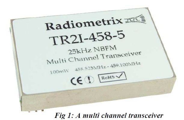
The ISM radio market still contains a very wide variety of module products, ranging from the very simplest short range, wideband units right up to high power, long range radio modems. About “half way up” the market, in terms of cost and sophistication, the keen observer will have noticed a shift from predominately single channel radios to multi-channel designs. The merits and problems of single versus multiple channel operation have been discussed elsewhere, but an issue remains worth discussing: how does a multiple channel module generate it’s (programmable) range of operating frequencies ?
Basic radio circuit theory points us easily towards the configuration necessary for single channel operation: a sufficiently stable oscillator (using a crystal, surface acoustic wave resonator, or just possibly lumped LC components depending on the degree of stability required at the operating frequency) is designed to operate on the required transmit (or receiver local oscillator) frequency. Sometimes, when the desired frequency is higher than the chosen oscillator technology can achieve, a sub-multiple of the wanted frequency is chosen, and frequency multiplier stages are included, but the basic principle remains the same: a single fixed frequency oscillating element defines the channel frequency.
When a different channel is desired, a new oscillating device is needed (older multiple channel radios frequently used switched banks of crystals to provide a limited range of channels, but this clumsy technique is rarely seen today).
A modern multiple channel design is quite different. The defining ‘local’ oscillator needs to be capable of moving from one channel frequency to any other, under user control. In most cases this is achieved by using a circuit configuration known as a ‘phased lock loop frequency synthesizer’.
The basic PLL is familiar to most engineers: The output of a phase comparator controls the tuning input of a variable frequency oscillator (a VCO) via a low pass “loop filter”. One of the phase comparator inputs connects back to the oscillator output, while the other is connected to an external signal source. Provided the tuning range of the VCO is not exceeded, it’s frequency will be ‘locked’ to the frequency of the external signal.
The frequency sysnthesizer adds two important element to this. The ‘external signal’ input to the phase comparator is derived from an accurate, fixed, “reference frequency” (Fc), and a programmable frequency divider (a ‘divide by N’) is placed between the VCO output and the phase comparator. The VCO frequency thus locks to N times Fc.
In the radio application, a second divider (the “R divider”) is used to generate the necessary reference frequency from a high stability crystal oscillator, and the local oscillator signal is taken (via suitable buffers) from the VCO output. The reference frequency is set to be the smallest frequency step that the local oscillator will need to be tuned by (usually the channel spacing of the radio).
F(VCO out) = N x F(reference) / R
Example: A simple ISM band transmitter operates over 433.9 to 434.65MHz
Channel spacing is 25KHz (30 channels)
A 13MHz TCXO provides the frequency reference.
So: Fc = 25KHz, R divider will need to be set to 13MHz/25KHz = 520 And: For output frequencies 433.9 to 434.65MHz:
the N divider will be set to values between 17356 and 17386
There is, of course, more involved in a practical frequency sysnthesizer implementation. On the one hand the N divider, R divider, the phase comparator and other ancillary circuitry are usually combined in a single integrated circuit, and in “single chip radio” devices, this synthesizer block is further combined with the VCO (and the rest of the radio’s circuitry) to simplify the designers task even more (at the cost of greatly reduced performance, especially in terms of oscillator noise).
On the other hand, there are many more constraints on the design than I have detailed above: The VCO must be designed for low phase noise (no easy task in itself) while still having sufficient tuning range for the phase comparator output voltage swing, and it must be buffered and isolated from the influence of the remainder of the radio.
Reducing Fc to tune in finer steps increases the settling time of the loop, and the inherent phase noise output rises too (as Fc is reduced, N must increase, and the loop multiplies any noise on the reference oscillator or dividers, by this factor too).
If an FM or FSK transmitter is considered, some means must be provided to modulate the output frequency (a subject that deserves an article of it’s own)
And the ‘single loop’ PLL synthesizer I’ve briefly described is far from the only configuration possible. There are multiple loop designs (frequently found in signal generators), designs using various fractional divider configurations, and hybrid PLL / direct digital synthesizers, to name but a few.
So why is any of this theory relevant to the user of a wireless module? Beyond intellectual curiosity, there are several good reasons:
And one day, you may need to design your own. Good luck!
By Myk Dormer for Radiometrix Ltd
First published in Electronics World Magazine.